TAB Vacuum Tube Audio Book Archive
In 2011, TAB Books published The TAB Guide to Vacuum Tube Audio: Understanding and Building Tube Amps. This book is available for purchase from the Book Store page.
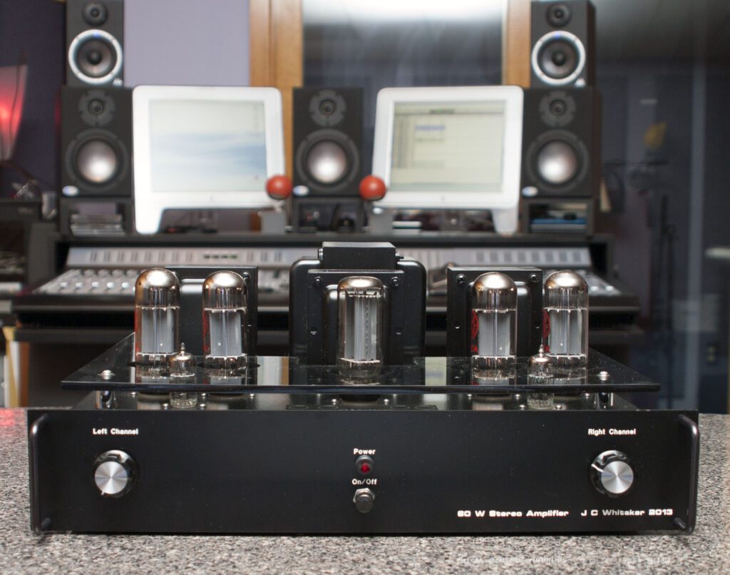
This blog supports The TAB Guide to Vacuum Tube Audio in a number of ways, including the following:
- Parts list for the projects described in the book as downloadable Microsoft Excel files
- PCB layout resources
- Additional supporting information and commentary on the projects contained in the book
- Corrections and errata from the first printing
- Other resources relating to vacuum tube audio applications
For more detailed information about the book see the Table of Contents and the Preface.

This book was written in 2010 and published in 2011. At the time, the only way to build a vacuum tube amplifier was to settle on a design, acquire the parts, prepare the chassis, assemble the unit, and test the final product. These steps are outlined in some detail in the book.
After the book was published, a revival of interest in vacuum tube amplifiers—driven in some part by a revival of interest in vinyl records—resulted in companies building new vacuum tube amplifiers for consumers, both in assembled and kit versions. The kits can be found for sale in any number of places—Amazon and eBay, to name just two. These kits appear to be of high quality, and generally speaking are inexpensive compared to the build-it-from-scratch option. The good news is that audio enthusiasts have many options now with regard to building a vacuum tube amplifier. People who want to build it from scratch can still do that, of course.
This blog serves as an archive resource for readers. It has been up for more than a dozen years; at some point the post will come down. Until then, we hope the resources here will helpful to builders of vacuum tube amplifiers.
Corrections and Errata
Unfortunately, errors can creep into a book as it works its way through the writing, editing, production, and printing process. The following items are known issues from the first printing:
- Page 56, Figure 3.5. Two traces are given for three different cathode temperatures. The upper curve for each trace should be dashed, as described in the figure cutline. This replacement figure shows the dashed lines correctly.
- Page 61, first equation on the page: some weird font issue is at play here. The equation should read mu = delta Eb divided by delta Ec1.
- Page 61, fourth equation (total cathode current of an ideal triode) is missing the quantity K (a constant determined by tube dimensions). The quantity inside the brackets is multiplied by K. When K = 1, the term falls out. The corrected page 61 equations are shown here.
- Page 69, Figure 3.17; disregard the dot on the plate (no idea where that came from).
- Page 73, at the bottom of the page the last line says “heather-cathode” it should read “heater-cathode”.
- Page 191, the last sentence on the page explains that pins 3 and 6 of the 5651A should not be used; the sentence reads “5615A” but should read “5651A”.
- Page 202, the text describing the Final Power Supply Design refers to an “R24”; it should be “R23” (there is no R24 on the parts list or on the schematic).
- Page 262, Figure 10.5, the terminal post “RVHa” should read “5VHa.”
- Page 311, paragraph 7 (counting the numbered list), the third sentence reads “Table 8.7 list typical…”; it should read “Table 8.6 …”
- Page 312, Figure 12.11 lists the tube type for V2 incorrectly as “7876.” This, of course, should be 7868 as described in Chapter 11.
Comments from the Author
The classic RCA Receiving Tube Manual (1975) served as a starting point for the circuits used in the projects described in the book. In most cases, tweaks were found to make the circuits work better. In all cases, complete parts lists were developed (which, for decades-old circuits, was not always easy). Why start with the 1975 edition, rather that some other edition? Well, it seemed like a good place to begin the effort since by 1975 receiving tube technology had arguably advanced about as far as it was going to, faced with very stiff competition from the transistor and integrated circuit. Improvements would certainly continue to be made (and are even still being made today), but it is evident that by 1975 tube technology had reached a very mature state. One could argue about the best “era” for tube development, but I’ll leave that for another forum.
The original idea when I began the book was to utilize vacuum tubes for the audio chain and current-technology devices and circuits for supporting systems. For example, solid-state (in some cases switching) power supplies, Op-Amp-based preamplifiers, and LED metering. After going down that road for a short period, I realized that a better approach would be to simply focus on the basics and attempt to build ’em like they used to. Readers can, of course, integrate new technologies into the basic designs described in the book if they wish. I didn’t go that route, however.
Another basic principle that I developed early on was that hiding the tubes within the chassis made no sense whatsoever. Let’s face it, part of the attraction of a vacuum tube amplifier is that you can see the tubes. Appearances are important in audio gear.
From the outset, I wanted to do in print what experimenters and hobbyists do in practice—namely, start with a basic circuit, built it, and then refine it. That seemed more interesting than just saying, “built it like this.” The other point here is that different things are important to different people. In online discussion groups you will find folks who claim that a tube amplifier should only be built a certain way, or only with certain tubes. I don’t subscribe to that. If you are happy with what you have built, who can possibly say you should have done it differently?
I want to stress this book was intended for the do-it-yourself hobbyist. It is not a book for audiophiles looking to build the ultimate audio system. A number of books have been published for the audiophile; this book is not one of them. Likewise, it is important to note that this book does not discuss guitar (and other types of music) amplifiers. Here again, there are a number of excellent books on that subject and interested readers are directed to those. The intent of the TAB Guide to Vacuum Tube Audio is to help hobbyists who want to build a tube-based amplifier do so. Pretty simple premise.
Hand-Wired or Printed Circuit Board?
That’s a good question, and I suggest the answer is “it depends.” In Chapter 5 of the book (in particular Table 5.1) some of the trade-offs with regard to hand-wired construction using terminal strips and printed circuit boards (PCB) are discussed.
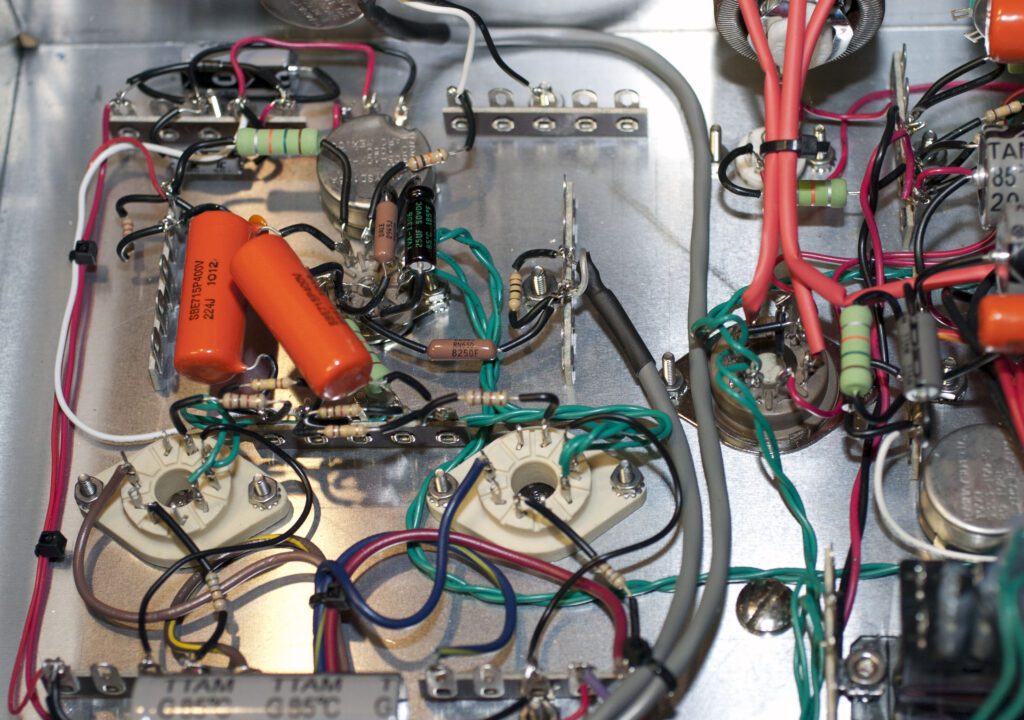
As described in the book, all of the projects began as hand-wired terminal strip-based implementations. This approach is ideal for one-off products and prototypes as it allows for rapid construction and facilitates change without too much difficulty.
For best performance, careful planning of component layout for a hand-wired unit is important. It is, for example, far easier to optimize a layout on paper than with a soldering iron. For that reason an accurate layout of the circuit components is advisable. This requires some amount of time, even if only done freehand as opposed to using a computer a drawing program.
As described in the book, PCB designs also require time to develop, and often require additional time to optimize. The real benefit of a PCB comes when multiple copies of a particular product or circuit are needed. Audio equipment usually has a built-in minimum multiple of 2 (stereo).
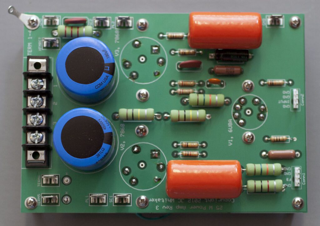
When working on the first versions of the circuits described in the book, my expectation was that I would build only one of each unit. After building one, however, I decided to build another to put in my office, and then my brother wanted one for his home, and then a friend dropped broad hints about how he would like one too. So, at a certain point, designing a PCB seemed like a good idea. It also provided an interesting challenge. (The challenge is, after all, a big part of the fun of building something.)
A middle ground between hand-wired terminal strips and a PCB can be found in the turret-type circuit board (also described in the book). Here again, advance planning is advised. The turret-board approach has found good applications in countless projects—large and small.
One could argue that for a hobbyist, there really is no right or wrong way to go about building something. If it works correctly, meets the intended application, operates safely, is reliable, etc., then by definition it was built correctly. Personal preference comes into play at all levels of an audio project. So, coming back to the original question “hand-wired or circuit board”, the answer is “it depends on how you want to build it.”
PWB or PCB?
Well, I don’t really care, but when writing the book I needed to pick one. Printed circuit board (PCB) is more commonly used to describe a method of component interconnection, but “PCB” also is an acronym for Polychlorinated Biphenyls, a very nasty substance widely used as an insulator in high-voltage electrical equipment, and subsequently banned because it causes cancer. A Google search of “PCB” brings up about an even number of results for circuit boards and outlawed substances. Printed Wiring Board (PWB) is accurate and descriptive, and does not risk confusion, which I admit is only a remote risk.
If you are more comfortable with PCB, please feel free to substitute it wherever you see PWB in the book. In defense of my choice, I believe that PWB stands the test of an acronym as it: 1) is defined, 2) is consistently used, and 3) minimizes the possibility of confusion within a given domain. Having said all that, since finishing the book I have switched to PCB because that’s the term most people are familiar with.
Feeedback—Inverse or Negative?
Same as above. I needed to pick one. The terms “inverse feedback” and “negative feedback” describe the same process of returning an inverted (negative) sample of the output of a stage back to the input as a method of reducing distortion. The RCA Receiving Tube Manual (in the 1975 edition at least) describes this as “inverse feedback.” Other texts, including the classic volume Radio Engineering by F. E. Terman (McGraw-Hill, 1947, Third Edition) describe the same process as “negative feedback.”
So, as with “PWB”, please feel free to substitute “negative feedback” for “inverse feedback” where you see it in the book if that term is more familiar.
Not to dwell on this, but another term used in some circles is “degenerative feedback.” I really don’t care for that term, however, and so I haven’t used it. But, if you want to, that’s cool too.
Ultra-Linear Operation
The use of a screen tap at 40 to 50 percent of the full primary winding has been used for many decades in all types of audio gear. Commonly known as “Ultra-Linear” operation, the technique was patented in 1937 (Blumlein). This technique may be used in either a single-ended or push-pull output circuit. The primary benefit is a reduction, sometimes significant, in distortion. There is a power penalty for this mode of operation, however. For example, a pair of 7868 power pentodes operated with identical parameters, can produce in the neighborhood of 34 W power output with fixed screen voltage, whereas the same circuit may produce about 24 W power output in the screen-tap configuration.
There are other considerations, of course, that determine the best circuit architecture. But as a first approximation, ultra-linear operation will reduce distortion but also reduce maximum power output. As documented in Chapter 10 of the book, the tradeoff is often worth it.
Caution: High Voltage
For the last 20 years or so, experimenters and hobbyists have been focused largely on projects based on solid state circuits, which typically operate in the 5 to 15 V range. That’s a far cry from the 400 V (or higher) plate supply of a vacuum tube amplifier. As such, extra caution is needed. We all know that, but it is worth reminding ourselves of the potential dangers every time we apply power to a tube circuit on the bench.

Proper labeling of equipment is important for safety reasons. A number of “warning” signs are available from multiple vendors. One online vendor is safetysign.com. Among the items builders may want to consider are the following:
- “Warning Hazardous Voltages Inside”, item #J5335-AF
- “Danger Risk of Electric Shock”, item #J5305-AF
- “Danger High Voltage”, item # E3360
These warning signs have an adhesive backing so they can be directly applied to the equipment chassis.
There are other on-line vendors in this space. You may want to also check out emedco.com.
After the book went to press in 2011, the author continued to tweak the circuits and experiment with different implementation ideas. Those efforts are documented below, along with commentary from the author. For readers that have a specific question about the projects described in the book, please use the Contact Us form.
Note that the parts lists provided in the following sections contained valid stock numbers as of the date of publication (2011). Component availability changes over time, and so some substitutions may be needed based on current availability.
Note also that the application files provided below are from programs in use at the time of publication. Most newer versions of computer applications are backward-compatible, in that older file versions can usually read by current version software. However, this may not always be the case.
Project: Stereo Preamplifier
This section includes supporting information intended to assist in building the stereo preamplifier described in Chapters 9 and 12 of the book, along with commentary from the author. This page picks up where the book left off.
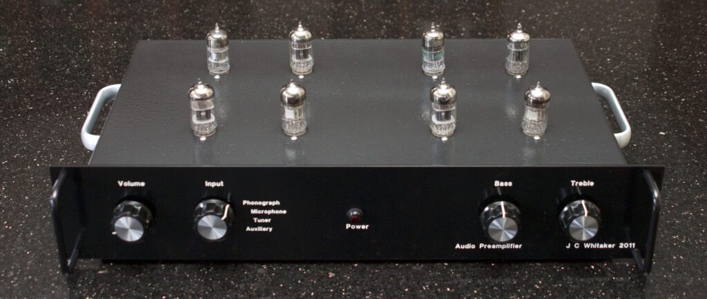
The stereo preamp serves as a perfect companion to the 25 W and 50 W power amplifiers described in the book. The preamplifier provides for four available inputs:
- Phonograph
- Microphone
- Auxiliary
- Tuner
An input switch selects the desired source, which is fed to a tone-control stage and finally to an output buffer amplifier. The final design includes a pair of printed circuit boards (PCBs) and stylized cabinet.
The starting point for the stereo preamp is a collection of preamp circuits described in the classic RCA Receiving Tube Manual (1975), with some new ideas and tweaks along the way.
One challenge in building a tube amplifier today is finding the right parts for the project. The bill of materials download below is intended to help make that effort easier.
The following documents are available for the stereo preamplifier, as a single ZIP file:
- Schematic diagram of the final design preamplifier (Figure 9.7 in the book).
- Bill of materials for one channel as an Excel spreadsheet (double the quantities for stereo).
- Printed circuit board layout as a “.pcb” (ExpressPCB) file for one channel (two boards are needed for stereo).
- Front panel layout design as a “fdp” (Front Panel Designer) file.
- Back panel layout design as an “ai” (Adobe Illustrator) file.
For those interested in using the PCB file, please remember that this file can be used only with the vendor ExpressPCB. The front panel layout file can be used only with the vendor Front Panel Express. See Chapter 9 and Chapter 12 for details on this project.
Note that the files above are provided as-is. Every effort has been made to make sure they are complete and accurate, but no warranties are expressed or implied. Builders are encouraged to double-check the information contained in the above files prior to proceeding. All files are provided for personal use only.
Note 1
The power amplifiers described in the book include provisions for running the preamplifier using B+ and heater voltages supplied by the amplifier. An industrial-grade connector is used for this purpose. The pin-out of the connectors provides for two separate ground connections for safety.
As an added measure of safety, it is recommended that a separate ground wire (#16 stranded is a good choice) be connected between the preamplifier chassis and the power amplifier chassis. This ensures that a solid ground is always maintained between the two devices. The simplest method of accomplishing this is to include a ground lug on the back panel of each chassis. The following sequence of components performs well in this application: #6-32 x 1-in screw / #6 lockwasher / chassis / #6 lockwasher / #6 locking nut / #6 flat washer / #6 wing nut.
A ground lug on the preamplifier back panel is also useful as a ground point for input sources, such as a turntable.
Note 2
It is important to note that the PCB designs developed by the author and available on this page are intended for tube socket mounting using standoffs as described in Figure 12.2 of Chapter 12 in the book. The PCB will not accommodate other mounting methods. An examination of the PCB design will show that the pads for the socket pins are evenly spaced around the perimeter of the socket. On the sockets themselves, however, the pins are not evenly spaced; there is extra space between pin #1 and the last pin (e.g., pin #7 or pin #9). This was done in order to provide for layout convenience on the PCB. With this approach, the maximum spacing between pads can be maintained, which makes it easier to place traces between socket pins while maintaining generous separation among components. The default layout separation is more than is actually required for the voltages typically present on the PCB. Readers who want to use socket mounting methods other than the one intended for the original design will need to reconfigure the socket mounting pads to match the method chosen. These cautions apply equally to the power amplifier PCBs.
Note 3
In Chapter 12, the procedure for making initial settings of the input level potentiometers is described. For the Auxiliary and Tuner inputs, an input level of 0.3 V rms is specified. This level works well for many inputs, notably an iPod/iPhone or similar device. Higher input levels may, however, be encountered with some consumer audio gear. For that reason, it may be advisable to set the Auxiliary input for an input reference of 0.3 V rms at 1 kHz, and set the Tuner input level control for an input reference of 1.0 V rms.
Note 4
As stated in Chapter 9 of the book, the microphone preamplifier is designed for use with a high-impedance dynamic mic. A low-impedance mic will work, but the output level will be low. For those wishing to use a low-impedance dynamic microphone with the preamp, a convenient solution can be found in the Sescom SES-LZHZ-XF14 “XLR Female to 1/4 Inch Male Low Z to High Z Impedance Matching Transformer.” This product (there are probably others that perform similar functions) works well with a variety of professional microphones. Tests by the author with a Shure SM58 showed good performance. The SES-LZHZ-XF14 is available from Markertek Online, and probably elsewhere.
While the stereo preamplifier described in the book used RCA jacks for the mic inputs, a 1/4-inch phone jack would be a better choice, as high impedance mics typically use this interface. Low impedance mics generally use an XLR interface, which is provided with the Sescom product. The Neutrix NJ3FP6C-BAG is a good quality 1/4-inch panel-mounted phone jack (Allied stock no. 70088266).
When using a product such as the Sescom matching transformer, take care to keep the device away from magnetic fields, such as power transformers. A magnetic field can produce hum in the device. For that reason, a distance of at least 3-feet is recommended between the power amplifier and the matching transformer. This caution also applies to phonograph pickup elements, which may be subject to the same issues.
Note 5
An updated version of the stereo preamplifier described in the book has been completed. Changes from the original design include some new features, improved physical layout, and a new circuit board design. The goals were to increase the functionality of the unit and improve (lower) the noise floor. The basic circuit elements remain the same. Extensive use of the first unit has shown the design to meet the stated objectives and to operate reliably.
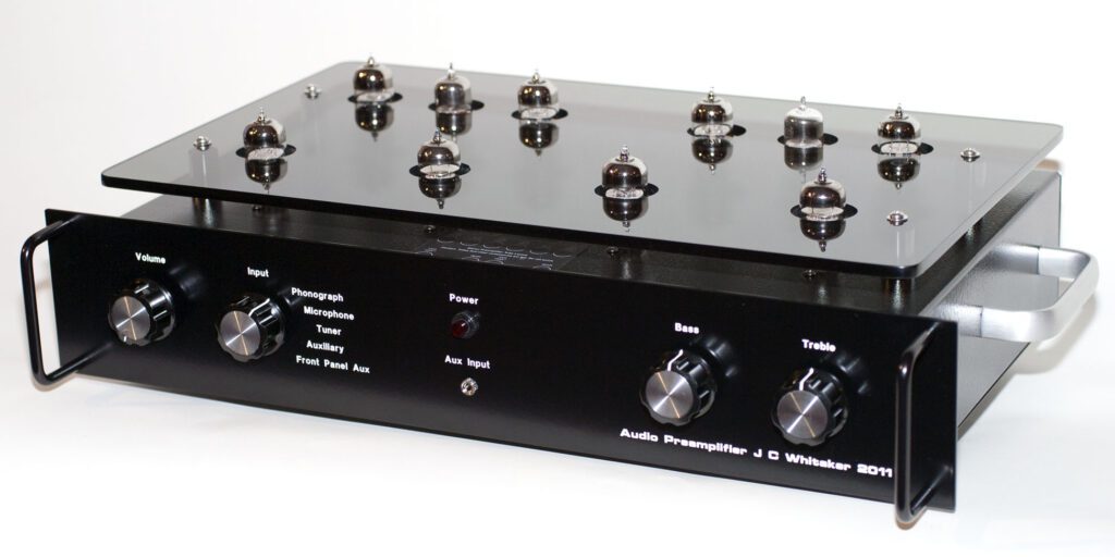
Specific changes to the stereo preamplifier include the following:
- Improved back panel configuration that simplifies the connection of source devices.
- Shielded cabling used for all board-to-chassis component connections. Also, better separation of left and right channel cable bundles.
- The addition of a “Tape Out” jack for each channel. This circuit taps the signal path before the tone-control stage to provide an output for recording on a separate device. The addition of a “Tape Monitor” switch for confidence monitoring was also considered, but it did not seem to be essential considering the challenge of finding room on the back panel for another pair of RCA jacks.
- A new PCB was developed that accommodates another buffer amplifier for the Tape Out signal and improves component layout. The design optimizes the the phono, mic, and tone-control stages and eliminates any signal-carrying traces on the component side of the board, which provides an unbroken ground plane over the component side.
- Removable connectors added for all off-board wiring. Previously, it was very difficult to remove a circuit board after it had been installed. The new design uses 10 plug-in connectors on each PCB.
- An improved, and simplified method of connecting the tube sockets to the board that reduces assembly time yet preserves the benefits of the first design.
Even with the design improvements detailed here, construction of this unit is challenging. But, the end result is quite nice. Details on this project are given in the following entries.
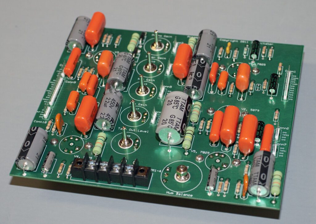
Note 6
During the course of building the second-generation preamplifier steps were taken to improve the high-end frequency response of the various inputs. Part of that work focused on the challenge of cable capacitance.
With any cable (two or more conductors, including shield), there exists a distributed capacitance. This capacitance is essentially constant along the cable and therefore increases as the length of the cable increases. A simple experiment was conducted using two common audio cables:
- Belden 8641 06100, a twisted pair, foil-shielded cable
- Alpha 1705, a single-conductor with a spiral-wrapped shield
Measurements were made to determine the impact of various volume control settings on the high-frequency response of the circuit, focusing strictly on the effect of the cable itself and the changing resistance of the potentiometer. Taken together, the series resistance of the potentiometer and the shunt capacitance of the cable forms an RC filter.
For the test, a 1 megohm linear potentiometer was connected to a 12-inch sample of each type of audio cable. An input signal was applied across the potentiometer ends, with the shield connected to the low side of the pot (ground on the signal generator). The center conductor of the test cable was connected to the wiper arm. An audio voltmeter (1 megohm input impedance) was then connected to the far end of the cable.
With this arrangement, various settings of series/shunt resistances could be examined. The results, detailed in table format, were revealing. As shown in the table, four settings of the potentiometer were measured. The setting with the greatest deviation from flat response was with 500 k ohm series/500 k ohm shunt, where response at 20 kHz was down 2.5 dB (relative to 1 kHz). The effect is more pronounced as the frequency is increased.
Note that the table also includes a “Baseline” column. This was essentially a test of the residual shunt capacitance of the audio voltmeter and the minimum measurable capacitance of the bridge. Focusing again on the 500 k ohm/500 k ohm “worst case” setting, the effect was negligible up to 20 kHz, although surprising large at 50 kHz. One could apply the Baseline readings as a correction factor for the test cable readings, and thereby subtract-out the effects of the instrumentation. This was not done in the table, which simply records the raw numbers.
The data demonstrate the importance of keeping lead lengths as short as possible, and the importance of using low-capacitance cable on high impedance circuits. Also, in order to maintain the same frequency response characteristics between channels in a stereo system, the cable lengths for a given function should be the same between channels.
Based on these experiments, some component value changes are suggested for the preamplifier described in Chapter 9 of the book. Referring to Figure 9.7 and Table 9.10 in the book:
- Change R16 and R17 from 1 megohm potentiometers to 250 k ohm potentiometers.
- Change R18 and R19 from 1 megohm potentiometers to 100 k ohm potentiometers.
- Change R32 from 1 megohm potentiometer to 250 k ohm potentiometer.
The circuit will certainly work well as described in the book. However, with the lower-value potentiometers, the adverse effects of capacitive loading from interconnecting shielded cable is reduced to a manageable amount; the typical series resistance is reduced by a factor of four for the phonograph and microphone stages, and for the buffer input stage. The changes in value suggested for R18 and R19 reflect the expected source hardware, which will likely be relatively low impedance devices.
As described in Chapter 9 of the book, the minimum load that the phonograph and microphone circuits should see is 220 k ohms. So, the 250 k ohm level controls present no problem for the circuit. The minimum specified load for the tone-control circuit is 100 k ohms; here again, the 250 k ohm Volume control works fine in this application.
Suggested part numbers for the replacement devices are given below:
- R16 and R17, 250 k ohm potentiometer, linear, Honeywell/Clarostat 308N250K, Allied stock #70153217
- R18 and R19, 100 k ohm potentiometer, linear, Honeywell/Clarostat 308NPC100K, Allied stock #70153229
- R32, 250 k ohm potentiometer, audio taper, Precision Electronic Components, KKA2541S28, available from DigiKey (and elsewhere)
Note 7
Another objective of the second-generation preamplifier was to reduce the noise floor. The major noise component of the first generation unit was 60 Hz hum. The minimum noise level of the stereo preamplifier described in Chapter 12 of the book was –60 dB. This is not bad, but not great either. Since the B+ power supply for the preamplifier circuits is taken from the audio power amplifier, in a separate chassis, the assumed source of the hum was the 6.3 V ac heater supply.
To determine the improvement that might be realized with a dc heater supply, the 6.3 V ac from the filament transformer was rectified by a full-wave bridge and filtered by a large-value electrolytic capacitor. The results were quite encouraging, lowering the noise floor by at least 10 dB. Tests conducted on the preamplifier showed the noise floor at –70 dB or lower (better) for all inputs.
The 6.3 V ac filament voltage is applied to a full-wave bridge rectifier (Vishay #6MB05A, Allied stock #70078708). The operating current pull from the preamplifier filaments is about 3.6 A. A 25 A rectifier is specified, however, because the Vishay 6MB05A provides a convenient mounting method (a single mounting screw) and when mounted against the chassis no additional heat sink is required. Filtering is provided by a 4700 microfarad, 50 V electrolytic (Illinois Capacitor #478TTA050M, Allied stock #70112239). When driving the 10 tubes contained in the stereo preamplifier, the output of the circuit is about 6.1 V dc.
Note that with a capacitor-input filter, the output voltage is influenced considerably by the load. Under no-load conditions, the output of a capacitor-input filter will rise to the peak level of the input ac waveform (1.4 times the rms level). Therefore, if a dc filament supply is used, do not operate the preamplifier with multiple tubes removed.
The impact of a dc filament supply on the life expectancy of the tubes used in this design, if any, will be hard to assess. Nonetheless, the author will keep an eye on this going forward. (Note: as of January 2024, eleven years after making this change, no tube failures have occurred.)
With the rectifier mounted against the chassis, the modification is easy to implement. No changes are made to the PCBs, and the Hum Balance control performs the same function as with ac on the filaments. The setting of the Hum Balance control has a surprisingly large impact on the noise floor when using a dc supply.
Note 8
Readers may recall that in Chapter 12, I mentioned that metal shields were not used over the phonograph and microphone preamplifier tubes. At the time I wondered how much of an improvement in the noise floor I might gain by adding shields. During final tests on the second generation stereo preamplifier I tried adding shields to the 7025 phono preamp and 5879 mic preamp tubes. With the dc heater addition there was no observable difference in the noise floor with or without tube shields. In all cases, the noise floor was well below –70 dB, relative to 1 V rms output from the Line Out jacks. Predictably, there was even less noise when measured from the Tape Out jacks, since the tone-control stage is bypassed when the Tape Out jacks are used.
Still, after a short search, I came upon some very stylish tube shields for 9-pin miniature sockets. These devices are bolt-on compatible with the Belton sockets specified in the parts lists contained in the book. The shields are available in a variety of colors, including yellow, red, green, blue, and black. Check them out on the Antique Electronic Supply web site. The shields cost about $1.50 each and look very nice. I have retrofitted the two preamps that I have built with these shields on the phono and mic input stages.
Note 9
The cost of building any project is an important consideration for the audio enthusiast and hobbyist. The focus of the first-generation stereo preamplifier was to optimize the various elements that went into the project. Cost was a secondary consideration. For the second-generation unit, an effort was made to accurately determine the bill of material (BOM) costs and the time needed to build the preamplifier.
The total BOM cost (including shipping expenses) for the second-generation stereo preamplifier was $1,570 (in 2015). The major cost centers included:
- Electronic components = $610
- Printed circuit boards = $320
- Tubes = $240
- Decals = $125
- Front panel = $100
- Plexiglas cover = $85
Builders could eliminate the PCB cost by using hand-wired terminal strip or turret construction. Other potential areas of cost reductions include the back and top-side decals, and the Plexiglas cover.
The total time required to build the second-generation stereo preamplifier—from ordering parts to completing performance measurements—was approximately 22 hours.
Note 10
The latest version of the second-generation stereo preamplifier is documented in the Vacuum Tube Amplifier Projects blog on this site. Complete construction details are available for download on the Available Downloads blog and a printed version of the user and assembly manual is available for purchase from the Available Printed Documents blog. If you are familiar with the Heathkit assembly manuals of the past, the approach taken with this manual should be easy to follow.
Considering the price tag, this project may be outside the range of some builders. However, you may find that elements of the available downloads will be useful in other projects, or wish to adapt some of the circuits for your own projects. The available documents are, thus, offered as a starting point for future efforts.
Project: 25 W Stereo Amplifier
This section includes supporting information for the 25 W stereo amplifier project described Chapters 10 and 12 in The TAB Guide to Vacuum Tube Audio, along with commentary from the author. This page picks up where the book left off.
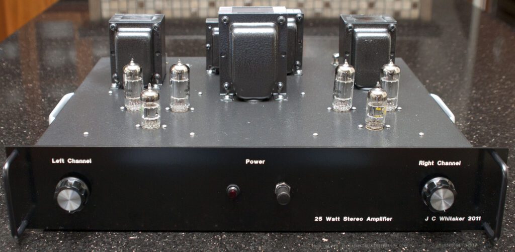
This amplifier provides approximately 12.5 W per channel. The input stage uses as 7199 pentode/triode and a pair of 6973 beam power tubes for the output section. This design is built around a pair of printed circuit boards (PCBs), one for each channel. A stylized cabinet is used, featuring exposed tubes. The starting point for this amplifier is a circuit described in the classic RCA Receiving Tube Manual (1975), with some new ideas and changes along the way.
This project is a good starting point for a a tube-based audio system. While not easy to build, it is not a huge project either. As with most tube-based amplifiers, the major costs are the transformers used in the project. The author has used Hammond transformers in this project and the 50 W amp described below with good results.
The following documents are available for the 25 watt stereo amplifier, provided as a single ZIP file:
- Schematic diagram of the final design 12.5 W amplifier block (Figure 10.4 in the book).
- Bill of materials for one channel of the amplifier as an Excel spreadsheet (double the quantities for stereo).
- Printed circuit board layout as a “.pcb” (ExpressPCB) file for one channel (two boards are needed for stereo).
- Front panel layout design as a “fdp” (Front Panel Express) file.
- Back panel layout design as an “ai” (Adobe Illustrator) file.
For those interested in using the PCB file, please remember that this file can be used only with the vendor ExpressPCB. The front panel layout file can be used only with the vendor Front Panel Express. See Chapter 10 and Chapter 12 for details on this project.
Note that the files above are provided as-is. Every effort has been made to make sure they are complete and accurate, but no warranties are expressed or implied. Builders are encouraged to double-check the information contained in the above files prior to proceeding. All files are provided for personal use only.
Note 1
The basic 12.5 W amplifier circuit of the final design implementation includes solid-state rectifiers for the B+ power supply. Mounting for these devices is accommodated on the PCB, as described in Chapter 10 and Chapter 12 of the book. At the reader’s option, it is possible to use a vacuum tube rectifier in place of the diodes. A 6CA4 tube functions well and matches the 9-pin style of the other tubes used in the amplifier. The 6CA4 is still being manufactured and is readily available. No changes to the PCB are required, other than routing leads that would go to the diodes to the tube socket. The original RCA design described in Chapter 10 of the book calls for a 5BC3 rectifier tube. This device will certainly work fine in this application, but it appears to be available only from new-old-stock (NOS) and can therefore be somewhat difficult to find. If a rectifier tube is used, be certain to route the B+ transformer secondary leads to the PCB and then, using jumper wires, to the rectifier socket. This is necessary in order to provide an input for the bias power supply. Operation of the circuit without proper bias will result in component failure.
Note 2
In the description of the 12.5 W amplifier in Chapter 10, the option of using a 6U8A tube in place of the 7199 as specified was discussed. The 7199 pentode/triode performs very well in this amplifier. The problem, however, is that the tube is no longer in production and finding NOS devices can be difficult (and expensive). As described in Chapter 10, it is possible to substitute a 6U8A so long as certain socket pin connection changes are made. The necessity to reroute three pins makes such a change difficult after the amplifier has been built, particularly if a PCB is used.
An interesting option involves a plug-in adapter available from at least one vendor that makes the necessary pin changes between the chassis socket and the tube. The adapter, shown below, is sold by Antique Electronic Supply (part # T-7199-ADT). The adapter is designed specifically for 6GH8A to 7199 applications. The 6GH8A is a medium-mu sharp-cutoff triode/pentode, as is the 6U8A. Fortunately, the pin changes needed to use a 6GH8A as a substitute for a 7199 are the same as for a 6U8A.
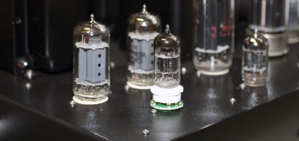
The author has tried the adapter on a 6U8A as a substitute for a 7199, with good results. Listening tests revealed no obvious differences between the tubes. Bench measurements followed.
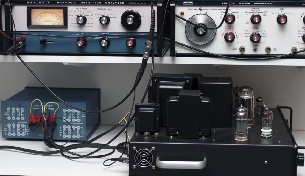
Measurements were taken on one channel of the amplifier with the 6U8A installed using the plug-in adapter. No significant differences were observed in frequency response, THD, IMD, or noise.
You will note that aesthetically the adapter may leave something to be desired in applications where the tube is visible. Still, it is an easy and inexpensive modification, and it avoids the difficulty of finding the 7199 type. The cost difference between a 6U8A and a 7199 is quite significant (in one case nearly a 10x difference). The larger question, however, is how long the 7199 will continue to be available—at any price. Therefore, having a backup type is important,
Following the successful tests of the 6U8A substitution for the 7199, tests were made on the 6GH8A as a substitute for the 7199, again using the 9-pin socket adapter. Listening tests were conducted that compared one channel with the 7199 and the other with the 6GH8A. No significant differences were detected. Bench tests showed performance comparable to the 7199 and the 6U8A.
It should be noted that some users have a preference for the sound of the 7199 over the lower-cost substitutes. The listening tests by the author as described here were not exhaustive. All other things being equal, the author recommends using the 7199. The problem, however is the difficulty of finding the 7199. At some point device availability must take precedence over preferences.
Note 3
The Bill of Materials for the 25 W stereo amplifier described in Chapter 10 of the book specifies a rating for circuit breaker CB1 of 5 A. This is actually higher than needed. Something in the 2 to 3 A range would be quite adequate. Builders may wish to try a 2 A device, such as the TE Connectivity W58-XB1A4A-2 (Allied Stock #70199386). If nuisance trips are encountered, a 3 A device may be used instead, such as the TE Connectivity W58-XB1A4A-3 (Allied Stock #70199433). Apart from the fixed load of the tube filaments, the bias setting on the final tubes is the major determinant of average power draw of the amplifier. At a bias setting of –30 V, the amplifier draws about 900 mA with no audio input applied.
As described in the Regulated Power Supply entry below, builders may want to change the value of VR1 to something higher than the 2.5 ohms (cold) specified in Chapter 12. VR1 is a power varistor intended to limit current inrush when the power supply is first switched on. Once the supply has reached operating temperature, VR1 is taken out of the circuit (shorted) by RYL1. A slightly higher value for VR1 will provide greater benefit. A value of 5 ohms (cold) works well with this circuit (GE Infrastructure Sensing #CL-40, Allied stock #70181325), limiting the measured inrush current to just over 3 A. With a 10 ohm (cold) device (GE Infrastructure Sensing #CL-60, Allied stock #70181341), the inrush current is reduced to about 2A. For builders who use a 2 A circuit breaker for CB-1 (which is recommended), the 10 ohm device is a good choice.
Note 4
Users may hear shortly after the amplifier is powered on a slight buzzing noise from the chassis (not from the speakers) for a few seconds. This is normal. As the amplifier warms up, the surge-limiting power thermistor bypass circuit of VR2 and C11 ramps up the voltage to relay RYL1. During a brief portion of this ramp, the relay may vibrate slightly; however, within a few seconds the relay will close. The speed of this action is a function of the ambient temperature.
Also, it may be observed that when the amplifier is first turned on, a faint hum can be heard from the speakers. This hum will go away within about 30 seconds of power on. Because the amplifier power supply uses silicon rectifier diodes, the B+ voltage is available immediately upon power up. This can allow any residual supply hum to be heard in the speakers. As the output tubes warm up and begin to conduct, the residual hum is canceled out by the push-pull output tubes (the residual noise is 180° out of phase). After the amplifier has warmed-up, the typical noise floor of –80 dB to –90 dB is achieved.
Note 5
An interesting condition can be observed with this amplifier when measuring square wave performance. Certain settings of the volume control provide for better square wave traces. To illustrate: Apply a 1 kHz signal to the input with the volume control fully clockwise. Adjust the generator to produce 8 V rms output at the speaker terminals into an 8 ohm load. Observe the trace displayed on the oscilloscope. Some ringing can be seen on the leading edge of the trace. Now adjust the volume control so that the ringing is minimized. This is usually around the 3 o’clock position. Readjust the signal generator to produce 8 V rms output at the speaker terminals. Note that the oscilloscope trace is clean.
The measurements documented in Chapter 12 of the book were based on this technique. Fortunately, very little listening is done at full-open volume control settings. This situation is a function of the characteristics of the input pentode stage, and was observed with both a 7199 and 6U8A tubes. In addition, a similar condition was observed with the 50 W stereo amplifier, which uses the same input pentode arrangement.
Note 6
A second-generation version of this amplifier was produced that incorporated several changes that were useful additions to the basic design. This amplifier is described as a 20 W stereo unit. Although each channel is capable of 12.5 W power output at low distortion, performance over time is unpredictable at maximum output. For this reason, the amplifier’s stated rating is conservatively specified.
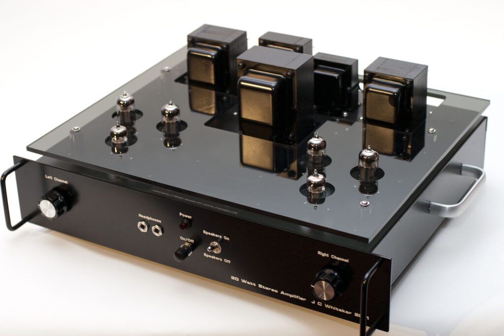
Version 2 of the amplifier, shown above, adds headphone jacks to the front panel and a speaker on/off switch. The speaker switch is used to mute the output at the speaker terminals when the headphones are used. To avoid running the output transformer secondary wires from the rear panel to the front panel, and back to the rear terminals, a pair of relays is included. The speaker on/off switch on the front panel switches a +5 V dc source (taken from the VR1 relay bypass circuit) to control the relays. When the relays (one for each channel) are energized, the 8 ohm secondary of each output transformer is applied to 8 ohm 10 W resistors.
The added headphone output was a feature suggested by a friend who wanted to use the amplifier for headphone listening, as well as for speakers.
The other major change, cosmetic in nature, was the addition of a Plexiglas cover over the amplifier, as shown. This gives the amplifier an interesting look and tends to protect the tubes from casual contact.
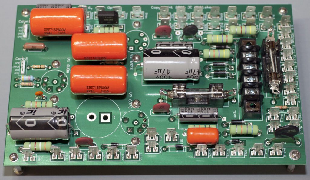
A modified circuit board was used that incorporates quick-disconnect terminals for connections to the transformers and other chassis-mounted components. The goal was to reduce the number of off-board connections in order to simplify construction.
The new PCBs feature a ground plane over the component side with a solder mask and silk screened legends. Two boards are used for the implementation; the power supply components are installed on only one board. In addition, a pair of speaker terminal PCBs is used to terminate the output transformer secondary windings.
The input stage uses a 6U8A pentode/triode, replacing the 7199 tube used in the original RCA circuit.
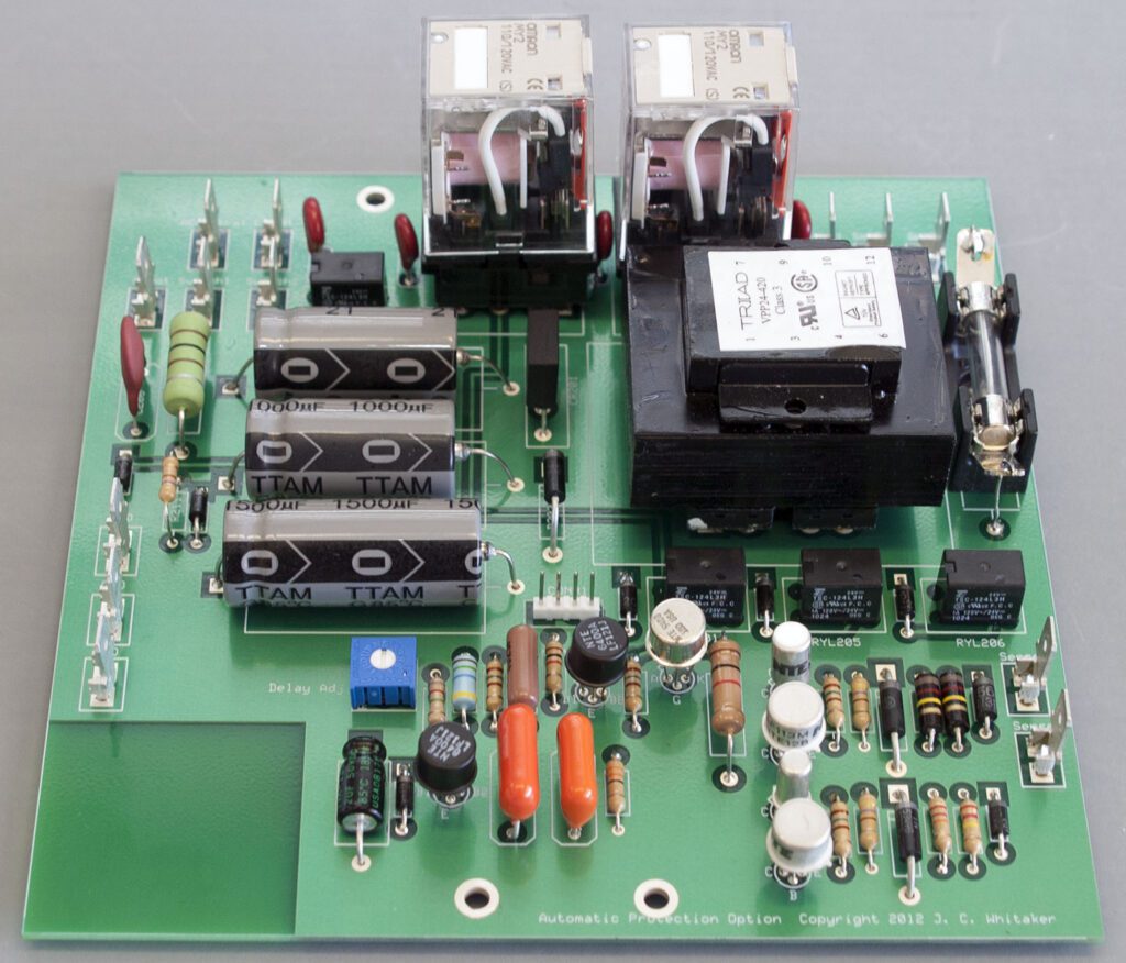
An new board, shown above, was incorporated in the the amplifier that adds several system-protection features including: automatic shutoff, over-temperature shutdown, and B+ under-voltage shutdown.
Note 7
The cost of building any project is an important consideration for the audio enthusiast and hobbyist. The focus of the first-generation 25 W stereo amplifier was to optimize the various elements that went into the project. Cost was a secondary consideration. For the second-generation unit, an effort was made to accurately determine the bill of material (BOM) costs and the time needed to build the amplifier.
The total BOM cost (including shipping expenses) for the second-generation stereo amplifier was $1,936 (in 2014). The major cost centers included:
- Electronic components = $510
- Transformers = $500
- Printed circuit boards = $455
- Plexiglas cover = $125
- Tubes = $110
- Decals = $75
- Front panel = $100
Builders could eliminate the PCB cost by using hand-wired terminal strip construction. Note that two PCB designs are used in this amplifier—one for each channel and one for each speaker output circuit, for a total of four boards. Other potential areas of cost reductions include the back and top-side decals, and the Plexiglas cover.
The total time required to build the second-generation stereo amplifier—from ordering parts to completing performance measurements—was approximately 21 hours.
The BOM cost for the optional auto-protect board was $686. The cost breakdown was roughly 50% for parts and 50% for the PCB. Construction time was about 2 hours.
As with any electronic product, costs fall rapidly as the volume (number of units produced) increases. For a one-off project, however, there are are not many ways to reduce the cost without reducing the feature set.
Note 8
The latest version of the second-generation 20 W stereo amplifier is documented in the Vacuum Tube Amplifier Projects blog on this site. Complete construction details are available for download on the Available Downloads blog and a printed version of the user and assembly manual is available for purchase from the Available Printed Documents blog. If you are familiar with the Heathkit assembly manuals of the past, the approach taken with this manual should be easy to follow.
Considering the price tag, this project may be outside the range of some builders. However, you may find that elements of the available downloads will be useful in other projects, or wish to adapt some of the circuits for your own projects. The available documents are, thus, offered as a starting point for future efforts.
Project: 50 W Stereo Amplifier
This page provides supporting information for the 50 W stereo amplifier project described Chapter 8 (the power supply), Chapter 11 (the amplifier board,) and Chapter 12 (complete system) in The TAB Guide to Vacuum Tube Audio, along with commentary from the author. This page picks up where the book left off.
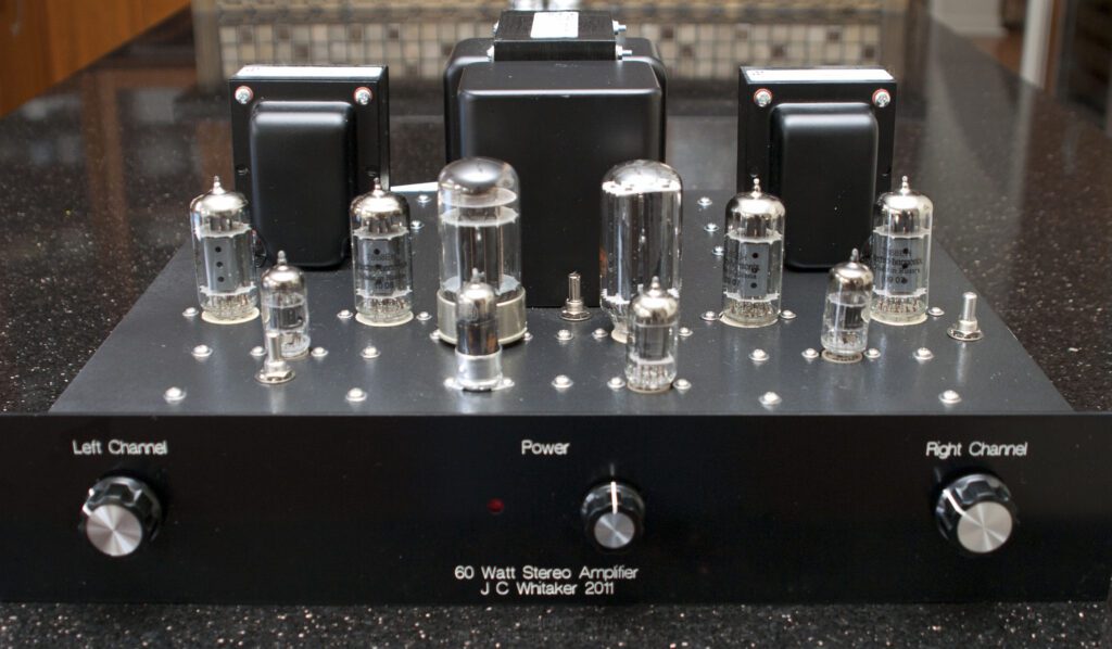
This amplifier builds on the 25 W stereo amplifier, using a high-capacity power supply and 7868 beam power tubes in a push-pull configuration. Exceptional performance is achieved through attention to detail and oversized output transformers. A great-sounding amp.
As with the other projects described in the book, the starting point for this amplifier is a circuit described in the classic RCA Receiving Tube Manual (1975), with some updates and modifications.
One challenge in building a tube amplifier today is finding the right parts for the project. The bill of materials download below is intended to help make that effort easier.
This is a relatively big project. Quality transformers are expensive, and the ones used in this design are no exception. Chapter 12 in the book describes construction of this amplifier as a hand-wired chassis. A PCB version has also been produced by the author, with good results.
The following documents are available for the 50 watt stereo power amplifier, provided as a single ZIP file:
- Schematic diagram of the final design power supply (Figure 8.6 in the book).
- Schematic diagram of the final design amplifier block (Figure 11.3 in the book).
- Bill of materials for one amplifier channel as an Excel spreadsheet (double the quantities for stereo).
- Bill of materials for the regulated power supply as an Excel spreadsheet.
- Printed circuit layouts as a “.pcb” (ExpressPCB) file: amplifier board, power supply board with regulator circuit, power supply rectifier, power supply regulator).
- Front panel layout design as a “fdp” (Front Panel Express) file.
- Back panel layout design as an “ai” (Adobe Illustrator) file.
For those interested in using the PCB files, please remember that these files can be used only with the vendor ExpressPCB. The front panel layout file can be used only with the vendor Front Panel Express. See Chapter 8, Chapter 11, and Chapter 12 for details on this project.
Note that the files above are provided as-is. Every effort has been made to make sure they are complete and accurate, but no warranties are expressed or implied. Builders are encouraged to double-check the information contained in the above files prior to proceeding. All files are provided for personal use only.
Note 1
The 50 W stereo power amplifier described in Chapter 12 of the book used hand-wired terminal strip construction (see below). After the book went to press, the author built another version of the 50 W stereo power amplifier using the PCB designs described in Chapter 8 for the power supply and in Chapter 11 for the amplifier.
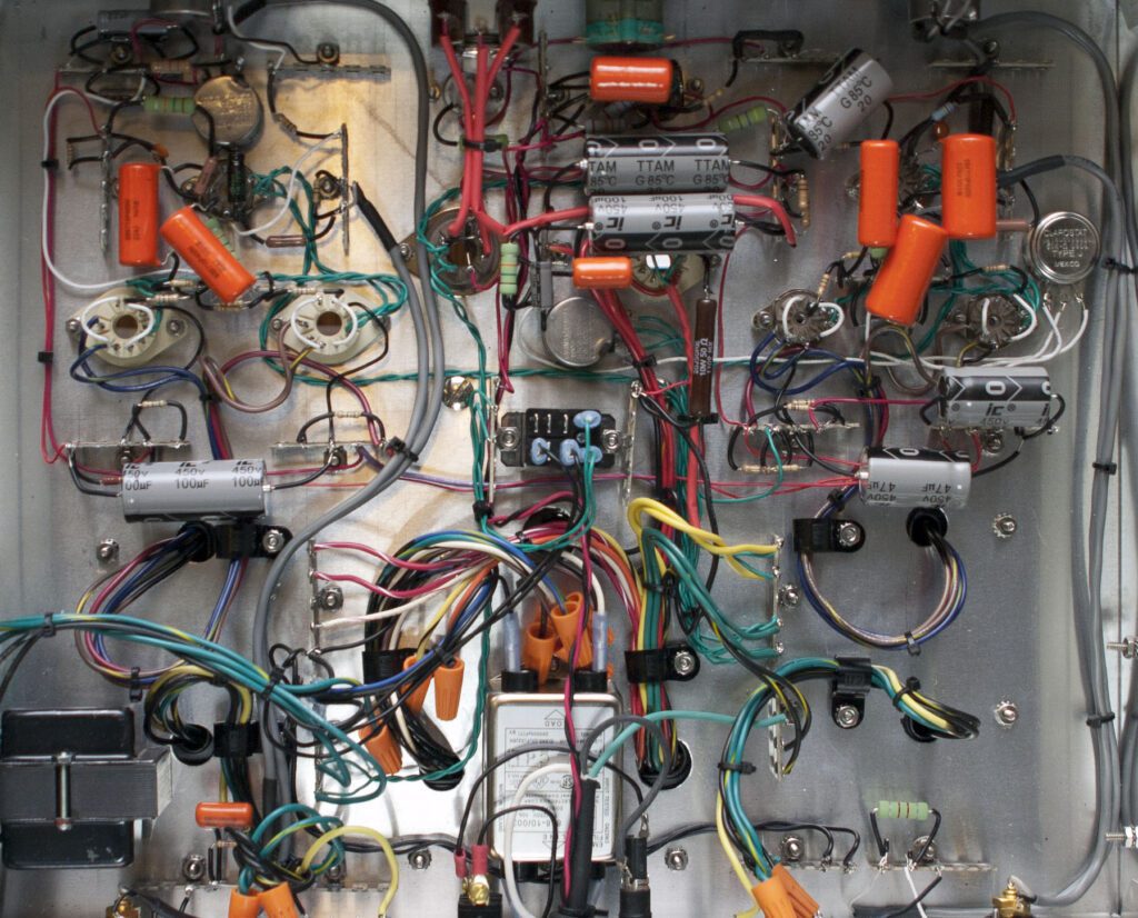
For the PCB installation using the board described in Chapter 11 and tube sockets specified in Table 11.7, it is necessary to use two types of standoffs to mount the sockets to the PCB. The 0.75-inch standoffs used in previous projects can be used for mounting V1 (the 7199 input/phase-splitter tube), but the 9-pin Novar sockets for the output tubes should be mounted on shorter standoffs (0.5-in). The same mounting considerations apply to the 5BC3 socket on the power supply PCB. When using the 0.5-inch standoffs on the 9-pin Novar sockets, it is necessary to pad the other standoffs to match the finished level of the Novar sockets. Two #4 flat washers are sufficient. It should be possible to add the washers and not exceed the minimum clearance limits of the PCB traces.
Construction of the power supply PCB is essentially identical to the design described in Chapter 8 of the book, with a few exceptions. Tubes V1 and V2 (5BC4 and 6080) were mounted directly on the chassis and connected with short pieces of hookup wire to the PCB socket pins. This was done in order to accommodate the large power transformer and choke used with the 50 W amplifier. The tubes will fit with the PCB design, but only with limited space between V1/V2 and the choke. To facilitate good cooling, a generous spacing margin was provided. For applications of the power supply PCB where all tube sockets are attached to the board (as designed), longer standoffs of approximately 1-inch are recommended to provide for adequate wiring space. Because the power supply circuits are essentially immune to noise concerns, the extra spacing has no material impact on performance of the circuits.
Note 2
The 50 W stereo power amplifier consumes all available space on the chassis. As a practical matter, this is about as big an amplifier as can built in a reasonably sized chassis. Beyond this point, dual mono block amplifiers may be the better approach. This amplifier is also quite heavy. The handles included on each side of the chassis are for more than just appearance. They are quite useful for moving the unit. The amplifier also generates a fair amount of heat owing to the beam power output tubes, rectifier, and series regulator tube. Normal convection cooling is adequate so long as airflow around the amplifier is not restricted by other devices, shelving, etc.
Because of the large number of interconnecting wires needed for this amplifier, expanded sleeving was used to organize the cabling. This tended to simplify cable routing and provided for a cleaner appearance. Wherever possible, cables were dressed either tight to the chassis, or well above the chassis so as to stay as far as possible away from signal-carrying lines and rest against the bottom cover plate, which further improved shielding. Because of the tight spacing of component elements, particularly on the power supply board, the order in which components and interconnected wiring were installed were important considerations.
Note 3
After building the 50 W stereo amplifier using PCBs, I had a difficult time completing the proof of performance while achieving the numbers expected. I was stumped by a distortion problem. The left channel amplifier performed very well—as expected—in all parameters (frequency response, noise, THD, and IMD). The right channel amplifier provided essentially identical performance in frequency response and noise, but THD and IMD were really bad. For example, at 20 kHz just below clipping, THD on the left channel was 1.6% but on the right channel it was over 6%. Both channels are identical; same design, same PCB layout, same parts. I tried switching tube sets, but the problem stayed with the sockets. In any audio amplifier, there are a few levers the builder can pull to make things look good, the easiest being the bias adjustment. But, no amount of bias setting on this amplifier would correct for 6% distortion (without the plates of the output tubes simply melting).
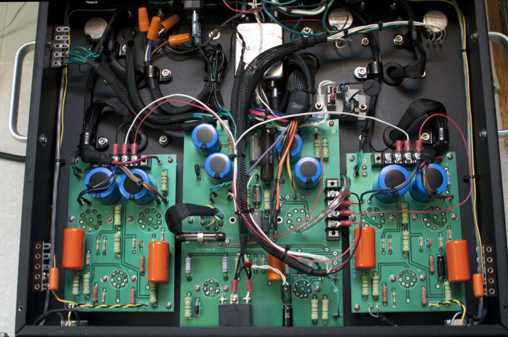
The underside of the chassis is shown above. After checking solder connections, component values, and ground connections for the nth time, I noticed that the channels are not completely identical. Because of the way the circuit boards lay out, the connection from the RC feedback circuit to the board is short on one side (about 2 inches) and longer on the other side (about 6 inches). For the left channel (the “long” one) I used a piece of shielded cable to connect to the board. On the right channel, I just installed a 2-inch piece of hookup wire. On a hunch (I had tried everything else), I replaced the 2-inch piece of hookup wire with a 6 inch length of shielded cable. And (you guessed it) distortion at 20 kHz just below clipping dropped from 6.5% to 1.5%. It seems there was just enough capacitance in the cable to influence the feedback circuit in a good way. I had built this amplifier before in a hand-wired (terminal strip) variation and did not have this problem. But, I had also placed the feedback RC components next to the speaker terminals and ran shielded cable (about 14 inches worth) to the input pentode cathode circuit. In the attached photo, you can see the RC components on each side of the chassis wired to terminal strips near the front panel.
So, the fix was to relocate the RC feedback components to the back panel of the chassis (next to the speaker terminals) and run shielded cable up to the front to the PCBs. Problem solved. Carrying the experiment a little further, I measured the capacitance of the shielded cable from the feedback circuit to the PCB terminals and then padded out the capacitor to compensate (about 30 pF). It didn’t make any noticeable difference in measured performance, but I felt better. One more suggestion: keep the lengths of the shielded cable the same for each channel.
Note 4
In Chapter 11 of the book, the option was discussed of substituting a 6U8A pentode/triode for the 7199 originally specified. As discussed above, the 7199 is becoming difficult to find (and expensive). The option of a substitute, therefore, has certain advantages. As documented in the book, the initial effort to substitute a 6U8A for the 7199 was not successful. Oscillations were observed at certain settings of the volume control, and as such use of the tube was not recommended. The implementation described in Chapter 11 was a hand-wired terminal strip design, and I wondered what the performance would be with the PCB-based layout. Returning to the 6U8A option, tests were made on the amplifier using the plug-in adapter detailed for the 25 W stereo amplifier. The results were quite positive.
The oscillations observed with the hand-wired implementation were not present with the 6U8A for the PCB implementation. Bench tests indicated essentially identical performance relative to the 7199. Tests were also made of the 6GH8A as a substitute for the 7199. Here again, bench tests showed no significant differences relative to the 7199, with the exception of THD at full power (25 W) where distortion at 10 kHz and to a lesser extent 20 kHz were about 1 percent higher than measured with either the 7199 or the 6U8A. Only a single 6GH8A was tried, so I cannot be certain this issue rests with the type of device or simply the device on hand.
Looking more closely at the oscillation issue initially observed, the first step was to examine the interelectrode capacitances of the two tubes, recorded in this table. Focusing on the pentode stage, the values for the tubes are closely matched. The oscillation did not occur at the minimum volume setting; not much of a surprise since the input is at near ground potential. The oscillation also did not occur at the maximum volume setting, arguably because that the capacitance of the cable to the back panel RCA input jack loaded the control grid of the pentode sufficiently to prevent the oscillation from starting up.
Testing this theory, with the volume control at an “oscillating” position, a 3.3 pF ceramic capacitor was connected between the 6U8A control grid pin and ground. The oscillation disappeared. It would appear that the adapter socket used previously exhibited just enough capacitance to prevent the oscillation. So, problem solved with a 3.3 pF capacitor between the pentode control grid and ground.
Looking at the oscillation problem from a different perspective, I was able to eliminate the oscillations and eliminate the shunt capacitor by changing the volume control potentiometer from 1 megohm to 100 kilohm. Since most modern input sources are well below 100 k, this is a simple and effective fix.
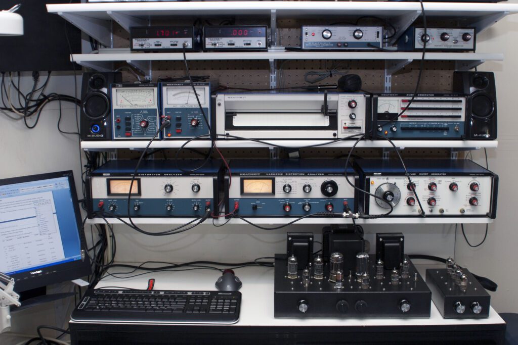
The photo above shows the 50 W amplifier on the bench undergoing performance testing.
The next step in the evaluation was listening tests with various types of program material. Results were mixed. A difference in the reproduced sound was observed, with a preference for the 7199. Having said that, the 6U8A worked well and reliably.
The 6U8A is a viable replacement for the 7199, although probably not the first choice. Critical listening tests were not conducted on the 6GH8A.
Note 5
The bill of materials for the 50 W stereo amplifier calls for an 8 A circuit breaker for CB1. However, a lower-rated device is quite adequate for this application. See the Power Supply section below. With an input line voltage of 117 V, the current draw is about 1.5 A with no signal input and no load connected to the auxiliary power supply socket.
Note 6
A new version of the 50 W amplifier has been completed, using the basic design and components described in Chapter 12 of the book. The major change in the new unit is the elimination of the power supply regulator circuit, which is not strictly necessary for operation of the amplifier. This change reduced the bill of materials cost by several hundred dollars, reduced the weight of the amplifier by about 8 pounds, and reduced the heat produced during operation.
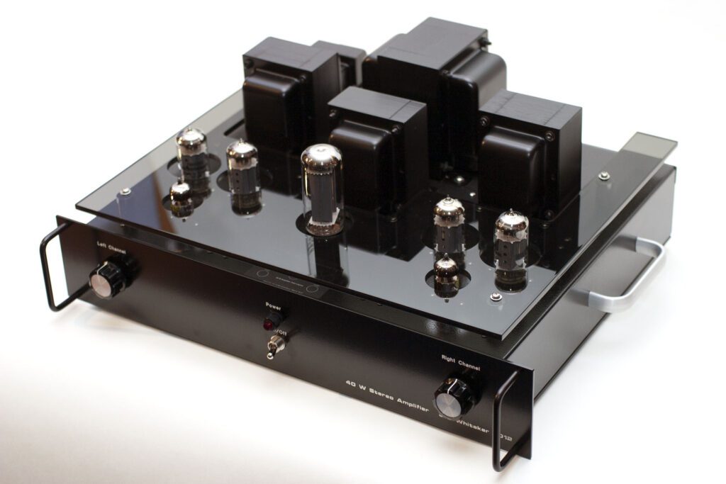
The photo above shows the completed amplifier. This implementation is described as a “40 W Stereo Amplifier” in recognition of the difficulty of getting a full 25 W power output from each channel when using the ultra-linear operating mode (output transformer screen taps) with acceptable distortion levels. At optimal bias settings, the amplifier is below 1% THD and IMD at 20 W output. Full-power frequency response is 10 Hz to 35 kHz (within 1 dB).
As mentioned, the power supply was modified from the previous version to eliminate the regulator circuit. Also, the 5BC3 rectifier tube was replaced with a 5U4, which is more readily available.
As with the other second-generation power amplifier, this unit includes a decorative acrylic cover, which serves to protect the tubes (and protect users from the hot surfaces of the tubes).
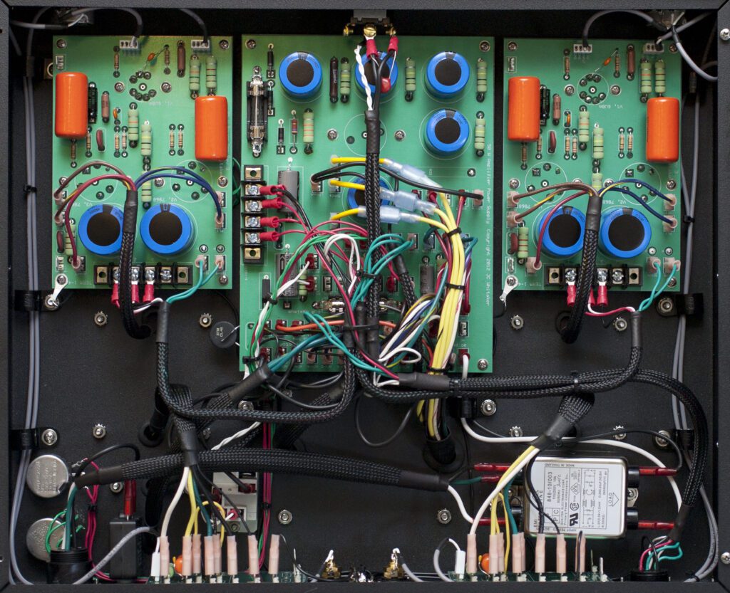
A total of five printed circuit boards are used in this implementation. The new power supply board incorporates connection points for all primary circuits, which simplifies construction considerably. A new amplifier board (two are used—one for the right channel and one for the left channel) was designed for the 6U8A input tube. Two speaker terminal PCBs are used, one for each channel; they serve to terminate all secondary leads from the output transformers.
Expandable nylon sleeving is used for cable management, in particular the primary and secondary transformer leads. Quick-disconnect terminals are used on all boards. This permits a PCB to be removed for service without the necessity of unsoldering wires.
As with the previous implementation, an auxiliary power connector is provided to drive the stereo preamp described in Chapter 12 of the book.
Performance of the amplifier is quite good—essentially identical to the 50 W unit.
Note 7
While working to optimize the performance of the second-generation amplifier, some adjustments were made to the feedback circuit that have proved to be helpful in reducing THD and IMD, particularly at high power levels. The original values for the resistor/capacitor feedback devices (R16/C6 in Figure 11.3 of the book) were 270 ohms and 0.01 microfarad, respectively. With the benefit of additional consideration, for circuits using the 6U8A tube for the input pentode/triode, it is suggested that R16 be changed to 200 ohms 0.5 W, and C6 be changed to 0.015 microfarad 200 V or so. The following parts are recommended:
- Vishay Specialty Capacitors, 0.015 microfarad, 200 WVDC, part #715P15352JD3, Allied stock #70079360
- Dale/Vishay, 200 Ohm 0.5 W, part #RN65D2000FB14, Allied stock #70200273
It should be noted that with these values, the amplifier sensitivity is reduced somewhat—on the order of 0.1 V rms.
Note 8
Based on the good experience with the automatic protection board described above for the second-generation 20 W stereo amplifier, I retrofitted the 40 W stereo amplifier with the Auto-Protect board. The board includes several system-protection features: automatic shutoff, over-temperature shutdown, and B+ under-voltage shutdown. Because of the physical layout of the 40 stereo amplifier, it was necessary to design a new circuit board in order to yield a PCB that would physically fit in the amplifier. The end result is shown below.

The PCB measures 2.95-inches by 12-inches and mounts on the inside of the chassis adjacent to the left channel amplifier board. Quick-disconnect terminals are used for all connections to simplify installation and maintenance.
The chassis view with auto-protection option installed is shown below.
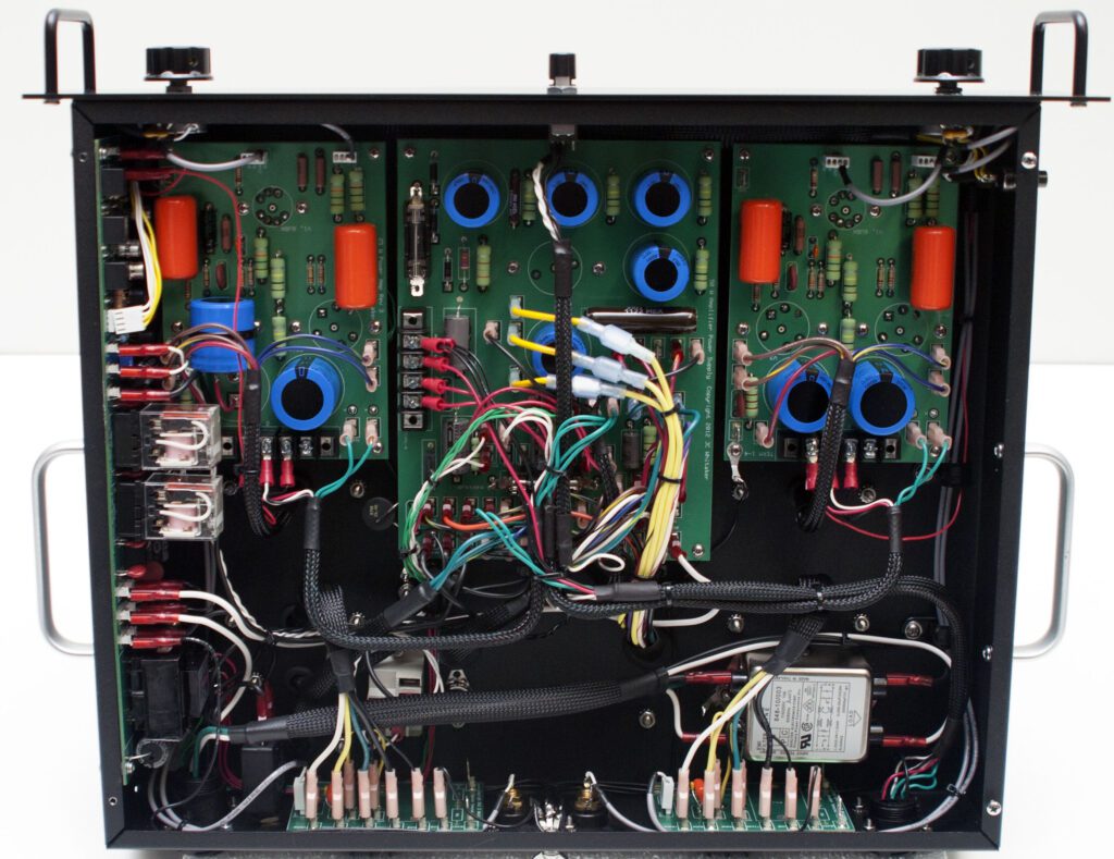
The automatic power-off feature can be enabled or disabled using a small switch placed behind the front panel on the right side of the chassis. In addition, an auto-off timer reset button is provided.
Note 9
The cost of building any project is an important consideration for the audio enthusiast and hobbyist. The focus of the first-generation 50 W stereo amplifier was to optimize the various elements that went into the project. Cost was a secondary consideration. For the second-generation 40 W unit described above, an effort was made to accurately determine the bill of material (BOM) costs and the time needed to build the amplifier.
The total BOM cost (including shipping expenses) for the second-generation 40 W stereo amplifier was $2,250 (in 2013). The major cost centers included:
- Electronic components = $540
- Transformers = $530
- Printed circuit boards = $650
- Plexiglas cover = $125
- Tubes = $165
- Decals = $75
- Front panel = $100
Builders could eliminate the PCB cost by using hand-wired terminal strip construction. Note that three PCB designs are used in this amplifier—one for each channel, one for the power supply, and one for each speaker output circuit, for a total of five boards. Other potential areas of cost reductions include the back and top-side decals, and the Plexiglas cover.
The total time required to build the second-generation stereo amplifier—from ordering parts to completing performance measurements—was approximately 22 hours.
The BOM cost for the optional auto-protect board was $686. The cost breakdown was roughly 50% for parts and 50% for the PCB. Construction time was about 2 hours.
Note 10
The latest version of the second-generation 40 W stereo amplifier is documented in the Vacuum Tube Amplifier Projects blog on this site. Complete construction details are available for download on the Available Downloads blog and a printed version of the user and assembly manual is available for purchase from the Available Printed Documents blog. If you are familiar with the Heathkit assembly manuals of the past, the approach taken with this manual should be easy to follow.
Considering the price tag, this project may be outside the range of some builders. However, you may find that elements of the available downloads will be useful in other projects, or wish to adapt some of the circuits for your own projects. The available documents are, thus, offered as a starting point for future efforts.
Project: Power Supply
This section includes supporting information for the regulated power supply project described Chapters 8 and 12 in The TAB Guide to Vacuum Tube Audio, along with commentary from the author. This page picks up where the book left off.
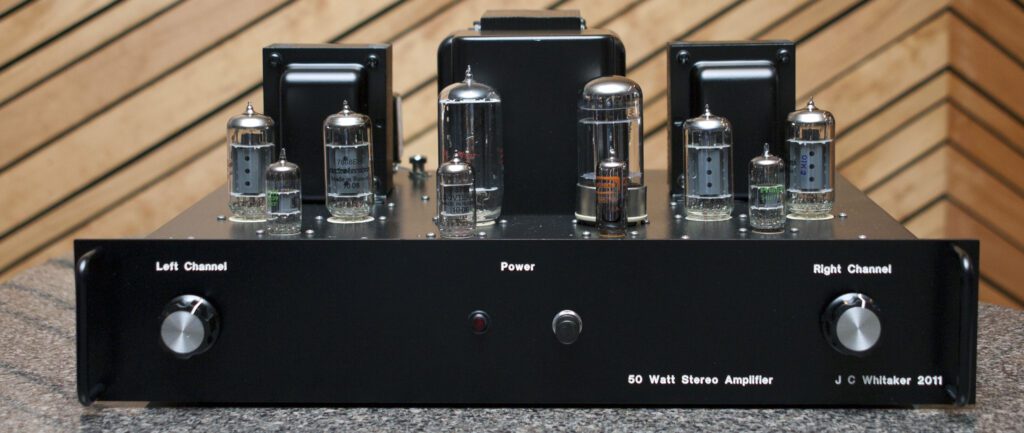
Shown above is the regulated power supply used on the 50 W stereo amplifier.
Note 1
A varistor may be added across the primary winding of the power transformer in order to minimize transient disturbance resulting from removal of primary power from the supply. Switches normally exhibit some amount of “contact bounce” when changed from one position to another. This can lead to noise resulting from the high voltages generated by the collapsing magnetic field of the transformers in the circuit. The varistor is essentially invisible in the circuit until a predetermined voltage is reached, at which point the resistance of the device decreases to a low value, thereby shunting the transient energy. Attention to transient disturbances is critical for proper operation of solid-state hardware; taking similar precautions in tube-based equipment is a good practice.
A variation on this approach is to place the varistor across terminals of the power switch rather than in parallel with the transformer primary. The net effect is about the same—a reduction in transient disturbances at turn-off (and to a lesser extent at turn-on). Analysis of any design needs to include the impact—if any—on safety should the device fail. In the case of the varistor, the usual failure mode is a short-circuit. That being the case, if the varistor failed the user would be unable to turn the amplifier off from the front panel. While this is an annoyance, it would not raise safety concerns under normal conditions. The author tried both approaches and each accomplish the objective of eliminating an audible pop or click when the amplifier is turned-off. This is an optional modification.
A typical device for this application is the V07E130P from Littlefuse, which is rated for 130 V ac (Allied stock #70184303). Make certain the varistor is placed after the ac line fuse or circuit breaker.
Note 2
As discussed in Chapter 8 of the book, be certain to use hookup wire rated for 600 V dc or above for the rectifier circuit of this supply. Common hookup wire is typically rated for 300 V dc, which is inadequate for the power supply rectifier and filters. Wiring for the voltage regulator can be rated for 300 V with the exception of the plate connections to the 6080 series regulator tube.
The current-carrying capability of the hookup wire used to build this power supply, or any other circuit described in the book or on this site, is usually not a limiting factor except when it comes to the primary and heater circuits. Generally speaking, hookup wire used in the primary circuit within the chassis should be no smaller than #18 (and properly fused). Heater circuits should use wire no smaller than #22; for power output tubes, #18 is usually a good choice. Keep the lengths of these wires to the minimum required by the physical layout. Specifications of standard copper wire for various wire sizes is given in this table (Source: Whitaker, J. C., AC Power Systems Handbook, 3rd ed., CRC Press, Boca Raton, FL, pg. 378, 2007.)
Note 3
The “final design” power supply described in Chapter 8 of the book (Figure 8.6) specifies a value of 8 A for circuit breaker CB1. This is more than is really necessary for the expected loads on the supply. A 5 A breaker (or even 4 A) should be sufficient. Consider the following parts:
- 4 A panel mount circuit breaker, TE Connectivity #W58-XB1A4A-4, Allied stock #70198794
- 5 A panel mount circuit breaker, TE Connectivity #W58-XB1A4A-5, Allied stock #70199427
The parts list for the final design power supply (Table 8.7) gives a value for VR1 of 2.5 ohms (cold). VR1 is a power varistor intended to limit current inrush when the power supply is first switched on. After the supply has reached operating temperature, VR1 is taken out of the circuit (shorted) by RYL1. Upon reflection, a slightly higher value for VR1 will provide greater benefit. A value of 5 ohms (cold) works well with this circuit. Consider using the GE Infrastructure Sensing #CL-40, Allied stock #70181325.
Note 4
In Chapter 8 of the book, Figure 8.6 shows the time-delay relay circuit used to short-out the ac input line varistor, VR1. This circuit consists of a 20 ohm (cold) varistor (VR2) in series with RYL1 (shunted by a large value capacitor) and a power source derived from an available 5 V ac winding on the power transformer. As designed, the voltage across RYL1 builds up as VR2 heats, eventually resulting in sufficient voltage across the winding to pull-in the contacts and take VR1 out of the circuit. The voltage at which RYL1 will activate is about 3.5 V dc. In the book, a pull-in time of about 60 seconds is estimated.
I have used this circuit successfully in many amplifier projects. It is important to note that the pull-in time is greatly influenced by the ambient temperature. In all of the implementations I have built, this circuit is contained within the chassis of the amplifier. Due to the other components within the chassis, the ambient temperature quickly rises to a point that the relay will pull in within a reasonable length of time. Having said that, the time delay will be longer on a cold day. For this particular application of the circuit, the actual delay time is of little consequence, since the only function of the relay is to short-out the thermistor in the input ac line. If it takes 30 seconds or 3 minutes to close, there is no impact on the performance of the amplifier. As such, the simplicity of the circuit outweighs the variability of operation. For a critical function, such as actuating some specific device, this circuit would be inappropriate because the pull-in time cannot be closely controlled.
A more sophisticated time-delay circuit could certainly be implemented. The one described in Chapter 8 continues to be used because it is inexpensive to implement and works reliably for the intended application.
Note 5
While checking out the Hammond web site for transformers for a new project, I came across a very useful “Design Guide for Rectifier Use.” See: http://www.hammondmfg.com/pdf/5c007.pdf. I hope you find this document helpful.
Trouble Log
This section focuses on the in-service reliability of the vacuum tube amplifiers described in The TAB Guide to Vacuum Tube Audio and detailed on this page. It is instructive to examine the failures in any system in order to improve the product and extend reliability. The following log details in-service reliability as of January 2024:
- First generation stereo preamplifier (described in the book): Placed into service February 2010. No failures. This preamplifier was decommissioned in 2022.
- Second generation stereo preamplifier (described on this page): Placed into service November 2011. No failures. This preamplifier was decommissioned in November 2024.
- Second generation 20 W stereo amplifier (described on this page): Placed into service December 2011. One failure—capacitor C9 in the bias power supply failed in a short circuit. Collateral damage was done to R17 and D2. Following an examination of the failure and parts specified, no changes were deemed necessary. Return to service one week later.
- First generation 50 W stereo amplifier (described in the book): Placed into service April 2010. No failures. This amplifier was decommissioned in November 2014.
- Second generation 40 W stereo amplifier (described on this page): Placed into service February 2012. One failure—the 6U8A input tube failed and was replaced. Returned to service one day later. This amplifier was bench tested in November 2024 and easily met the new product performance targets.
As with any consumer device, the amount of usage each product has experienced varies. Usage of these products can be reasonably described as equivalent to that of most any other audio product in a home.
Circuit Board Issue
Aside from the issues detailed above, there have been no additional failures from the projects covered in the book and on this page as of January 2024. There was a failure observed during tests on a new amplifier under development, however, that is worth reporting. As with any new circuit implementation, there is a troubleshooting period where problems (or potential problems) are identified and corrected. This is the reason, naturally, that building the first unit is always more time-consuming and expensive than building the second.
The downside to a problem is obvious—the system does not work or is otherwise impaired. The upside (or at least the potential upside) is to learn something from the failure that permits a more reliable system to be built—either from scratch or as a modification to an existing system.
Several years ago I began building a new amplifier. Based largely on the 40 W stereo amplifier detailed above, the new amplifier uses a different 6U8A input configuration and a considerably enhanced power supply. Operationally, the power supply changes are the core of the upgrades.
For the this amplifier, rated for 60 W output, a capacitor-input filter was used that developed sufficient B+ voltage to achieve 30 W per channel from the circuit. For any capacitor-input filter, the regulation from light load (idling condition) to full load (rated output) is poor compared to a choke-input filter. For the new amplifier, a choke-input design was used. In order to achieve the needed voltage for the output tubes, a Hammond #382X power transformer was used, which provides 1,000 V ac center tapped at 283 mA for the plate supply. Using a conventional full-wave rectifier circuit (center tap grounded) feeding a 5U4 tube, a calculated B+ voltage of 450 V dc was obtained at the output of the filter (the actual voltage was less due to losses).
The rectifier circuit was implemented on a PCB, as shown below.
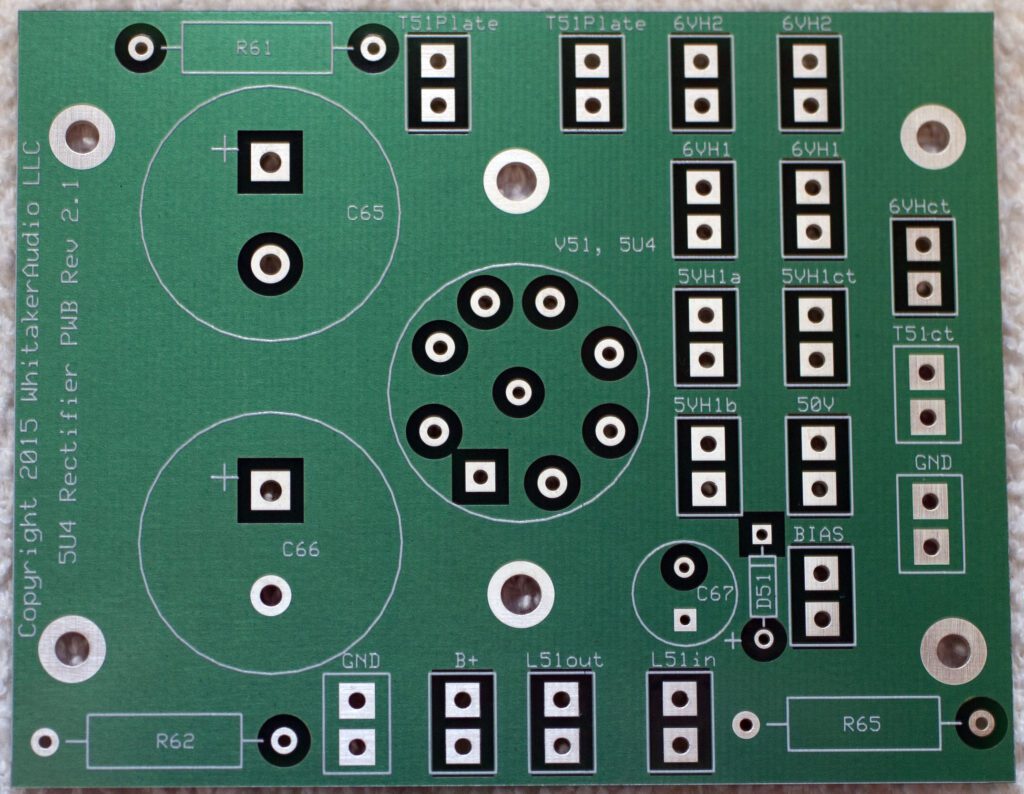
The amplifier was successfully built and ran on the bench and in a test environment for more than a month without issues.
Quite unexpectedly, one connection pad on the rectifier board failed, as shown in the photo below. The connection point is for the input to the choke (“L51in”). This was quite a surprise since the same board has been used in other amplifiers running higher voltages for a longer period of time without any issues. Even under no-load conditions (all tubes removed except the rectifier), the maximum dc voltage at L51in is no higher than 470 V. For the 40 W stereo amplifier the no-load output voltage on the same terminal is in excess of 560 V.

The first explanations that come to mind include a flaw in the circuit board itself, a voltage surge on the ac input, or some type of debris on or adjacent to the terminal. The last potential explanation may have been the cause, since the failure occurred a few minutes after service was performed on the amplifier on an unrelated board. No other electronic devices on at the time experienced a problem, which makes a transient disturbance on the ac line less likely. (It cannot be ruled out, however.)
A close-up view of the connection point in question on an unused board is shown below. The board uses a solid ground plane on the component side of the board. The boards are manufactured double-sided with all holes plated-through. The laminate is 0.062″ FR-4 epoxy glass with 1/2 ounce copper. FR-4 is a composite material composed of woven fiberglass cloth with an epoxy resin binder that is flame resistant (self-extinguishing). The top and bottom solder mask layers are green LPI (Liquid Photoimageable). A white silkscreen is printed on the top side of the board showing component outlines and text. The board finish is the industry standard SMOBC (solder mask over bare copper). The surface finish has two essential functions: 1) to protect the exposed copper circuitry, and 2) to provide a solderable surface when assembling (soldering) components to the PCB. The maximum operating temperature of the board is 125 degrees C. The default clearance around traces and pads is 0.05 inches, the maximum available with the ExpressPCB software.
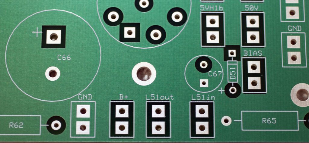
Focusing on the L51in terminal, the white outline is somewhat deceptive in that the silkscreen box is actually inside the cut-back area of the ground plane. As such, there is more insulating distance than might at first appear. The insulation distance from each terminal to the ground plane is the same in the horizontal and vertical directions (although it may not appear to be so from the photo).
In order to determine the practical operating stand-off voltage of the power supply circuit board, as built, an experiment was run. As shown in the photo below, two high-voltage power supplies—each capable of producing 400 V dc—were connected in series to provide 0 to 800 V dc. The negative lead was connected to ground plane of the board type that failed (shown above). The positive lead was connected to the L51out terminal on the board. This terminal is directly adjacent to the L51in terminal, where the short-circuit occurred. A voltmeter was connected to the board ground plane and the L51out terminal so the actual voltage applied to the board could be monitored.
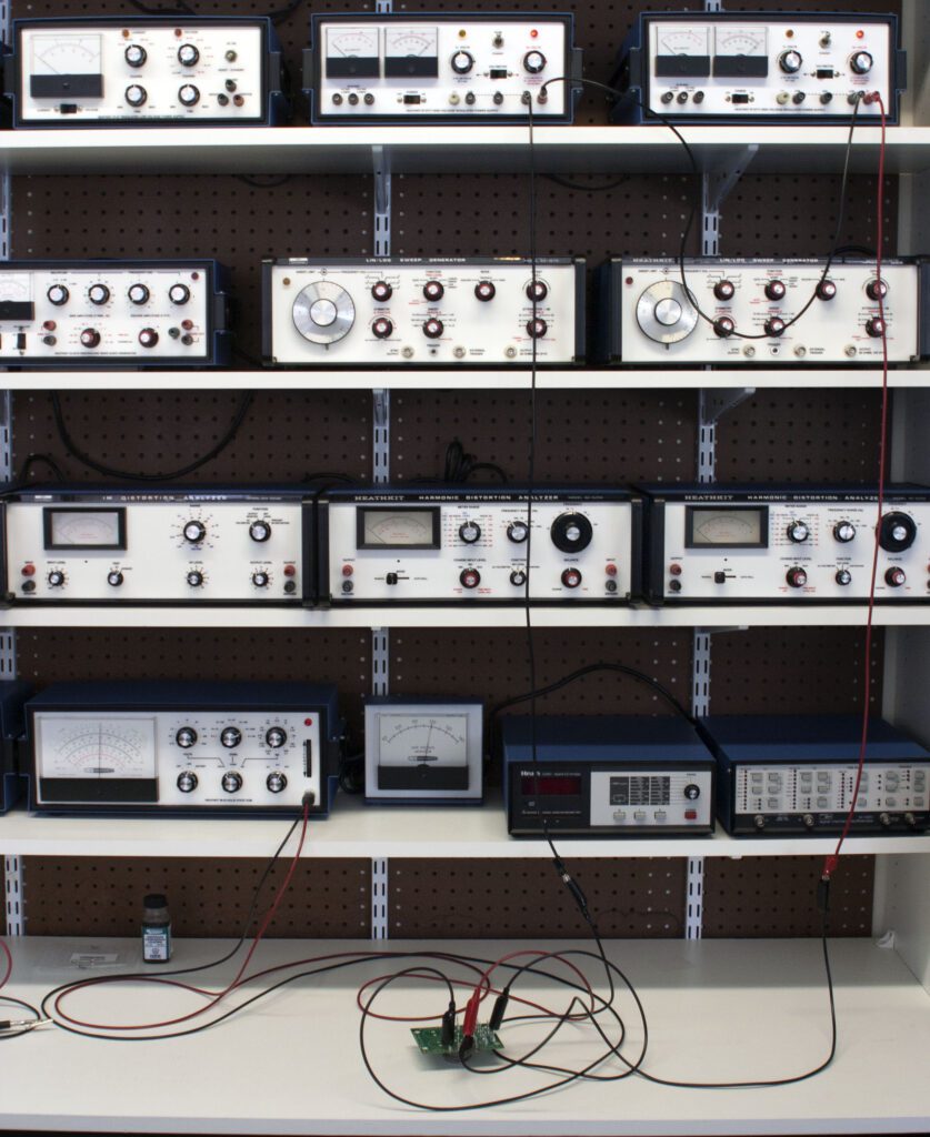
The goal here was to identify the maximum voltage that the circuit board could withstand before a flash-over failure occurred. Because the typical operating voltage at L51in (the terminal that failed) is 400 V dc, a test voltage of twice that (800 V dc) was deemed to be sufficient to confirm that the original design parameters were sufficient for reliable operation.
With the connections made, the voltage was ramped up while the current (as shown on the power supplies) was monitored. The voltage was successfully brought up to the maximum output of the supplies (800 V dc) with no observable problems on the board, and zero current as measured at the supplies.
So, with a minimum 2X operating margin, the most likely cause of the failure was determined to be one of the following (in order of likelihood):
- (1) Conductive debris on or near the terminal resulting from maintenance work performed shortly before the problem occurred.
- (2) A transient disturbance on the ac line, with the voltage surge acting in conjunction with the choke (5 H) in such a way to produce a voltage that exceeded the breakdown voltage of the PCB.
- (3) A manufacturing defect on the board itself.
Based on these conclusions, a plan could be devised to prevent a similar problem from occurring in the future.
If cause #1 led to the failure, the solution is simple—check for and remove any loose debris (clipped leads, etc.) in the chassis after any maintenance. Turn the amplifier in various positions to remove anything that might be lodged in a corner.
If cause #2 led to the failure, the solution is a little more complex. Transient disturbances are a fact of life. The amplifier already includes an ac line filter that will attenuate noise on the line, and to a lesser extent small transient disturbances. Metal oxide varistors are commonly available for protecting ac circuits. A varistor such as the EPCOS B72220S131K101 (130 V rms, 8 kA) should be quite sufficient. Because such devices are inexpensive, including one across the ac input to the amplifier (after the circuit breaker) is easily done. Such a device will be included on all amplifiers going forward.
Because the terminal on the PCB adjacent to the one that failed could hold off at least 800 V dc, a manufacturing defect is unlikely. However, as a general rule, I will begin applying conformal coating (see the section on Special-Purpose Chemicals on the Workbench blog) to terminals operating at 400 V or greater that are adjacent to a ground plane. One product that works well for this is the MG Chemicals 419C-55ML Acrylic Conformal Coating (2 oz bottle).
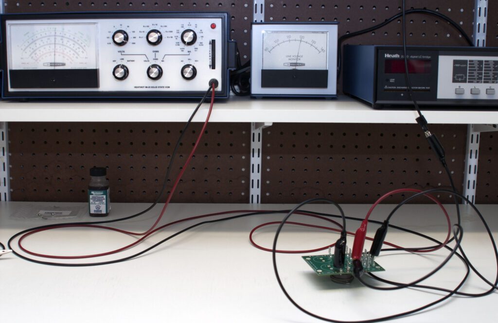
So, it is expected that this in-service failure will lead to more reliable systems in the future. One of the greatest challenges in engineering and design is anticipating things that might go wrong. Once you knave an idea of what might fail, it is then possible to take steps to mitigate the possibility of failure in the field.
Circuit Board Issue Update
It has been several years since the problem documented above occurred. The amplifier has been in use ever since without issues.
Following up on the voltage standoff concern, I came upon a newsletter article from ExpressPCB. The article discussed the maximum standoff voltage for typical circuit boards. A portion of the article is abstracted below.
“The dielectric material of our 2-sided PCBs should handle up to around 50 kV with respect to dielectric breakdown between layers. FR-4 material will absorb moisture out of the air but the solder-mask does a good job of limiting that through the largest surface areas, leaving only the boards edges. This absorption of moisture around the edges typically has very little effect on the dielectric breakdown voltage and may lower the 50 kV number to 45 kV (to be safe). The main issue where temperature and humidity might come into play is arcing between adjacent current-carrying circuits. With PCBs incorporating a solder mask, there are typically no issues with temperature or humidity from a voltage standpoint; the dielectric breakdown of our solder-mask has been tested to 2800 V/mil of thickness. Our typical thickness in and around the conductors is about 1 – 1.2 mils. This would allow for about 2500 – 3000 V before there might be any breakdown of this layer. For PCBs without solder mask, it is theoretically possible for an arc to occur between adjacent copper traces in high temperature, high humidity if the conditions and voltage are just right to overcome the breakdown voltage of the surrounding air.
The main concern of bare PCBs in a humid environment would be oxidization of the exposed conductors. Immersion silver finish has been known to oxidize if stored without environmental protection. We recommend that bare immersion silver boards be treated similarly to moisture sensitive components, sealing any opened bags, using desiccant, and protecting from UV light exposure. Boards shipped with the tin lead finish are not nearly as susceptible to these environmental concerns and can typically be stored for a year without issues. Once a PCB with solder-mask is assembled, the solder typically coats all of these exposed areas and the oxidation of solder is very low.”
In addition to the projects described in the book, the author has documented additional vacuum tube audio projects and posted them on this site. See the Vacuum Tube Amplifier Projects blog.